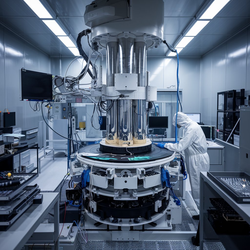
Extreme Ultraviolet (EUV) lithography has emerged as a groundbreaking technology in semiconductor manufacturing, enabling the production of smaller, more powerful chips essential for advanced electronics. As the demand for cutting-edge technology continues to surge, EUV lithography stands at the forefront of the semiconductor industry’s evolution. This article explores the future of the EUV lithography industry, highlighting its advancements, challenges, and potential developments.
The EUV lithography industry is expected to reach USD 25.3 billion by 2028 from USD 9.4 billion in 2023, at a CAGR of 21.8% during the 2023–2028 period. Extreme Ultraviolet Lithography (EUVL) is an advanced semiconductor manufacturing technique used to create integrated circuits (ICs) with smaller feature sizes and higher precision. It is considered one of the key enabling technologies for the continued miniaturization of electronic devices. The core component of EUV lithography is a specialized light source, mask, and optics. This source generates intense pulses of EUV light by converting a high-power laser beam into EUV radiation using a process known as laser-produced plasma. The EUV light is then directed onto a mask, which contains the pattern to be printed onto the silicon wafer.
Advancements in EUV Technology
EUV lithography operates at a wavelength of 13.5 nanometers, significantly shorter than traditional photolithography methods. This shorter wavelength allows for the fabrication of finer patterns on semiconductor wafers, crucial for the production of smaller transistors. As manufacturers push the limits of Moore’s Law, EUV technology is becoming increasingly essential.
Recent advancements in EUV technology have focused on improving throughput, resolution, and yield. Companies like ASML, the leading supplier of EUV lithography equipment, are continuously refining their machines to enhance performance. Innovations such as high-NA (numerical aperture) EUV lithography are on the horizon, promising even greater resolution and pattern fidelity. These advancements are critical for manufacturers aiming to develop chips with 3nm and smaller process nodes.
Growing Demand for Advanced Semiconductors
The global shift towards digitalization and the rise of technologies such as artificial intelligence (AI), 5G, and the Internet of Things (IoT) are driving unprecedented demand for advanced semiconductors. As devices become smarter and more interconnected, the need for smaller, more efficient chips is paramount.
EUV lithography enables manufacturers to produce highly advanced chips that meet these demands. Leading semiconductor companies, including TSMC, Samsung, and Intel, are increasingly adopting EUV technology to enhance their manufacturing capabilities. This trend is expected to continue, with more companies integrating EUV into their production lines to remain competitive in the rapidly evolving market.
Challenges in EUV Adoption
Despite its advantages, the adoption of EUV lithography is not without challenges. The complexity and cost of EUV equipment are significant hurdles for many manufacturers. The machines are expensive to produce, and the maintenance costs can be high, creating barriers for smaller companies or those with limited resources.
Moreover, the supply chain for EUV lithography is intricate. It relies on numerous components from various suppliers, making it vulnerable to disruptions. As seen during the COVID-19 pandemic, any disruption in the supply chain can lead to delays in production and increased costs.
Additionally, there are technical challenges to address. Achieving consistent performance and yield at the smaller process nodes requires ongoing research and development. The industry must also navigate issues related to mask defects and exposure strategies to maximize efficiency.
Download PDF Brochure @
https://www.marketsandmarkets.com/pdfdownloadNew.asp?id=241564826

Collaborative Efforts and Ecosystem Development
To overcome these challenges, collaboration among industry stakeholders is crucial. Semiconductor manufacturers, equipment suppliers, and research institutions are increasingly working together to drive innovation and share knowledge. Collaborative efforts can accelerate the development of next-generation EUV technologies and create a more robust ecosystem.
Public-private partnerships and industry consortia are also emerging to facilitate research and development in EUV lithography. These collaborations can help pool resources and expertise, fostering breakthroughs that will benefit the entire industry.
Future Trends and Innovations
The future of EUV lithography is set to be shaped by several key trends and innovations:
a. High-NA EUV Lithography
As mentioned earlier, high-NA EUV lithography is expected to be a game-changer. By increasing the numerical aperture, manufacturers can achieve greater resolution, enabling the production of chips with even smaller features. This advancement will be critical as the industry pushes towards 2nm process nodes and beyond.
b. Integration with Other Technologies
The integration of EUV lithography with other advanced technologies, such as machine learning and artificial intelligence, will enhance manufacturing processes. These technologies can be used for predictive maintenance, process optimization, and defect detection, leading to higher yields and reduced downtime.
c. Sustainability Initiatives
Sustainability is becoming a significant focus in the semiconductor industry. The EUV lithography process must evolve to minimize its environmental impact. Innovations aimed at reducing energy consumption, improving resource efficiency, and recycling materials will be essential as the industry seeks to become more sustainable.
d. Expansion Beyond Traditional Applications
While EUV lithography has primarily been associated with advanced semiconductor manufacturing, its potential applications are expanding. Industries such as automotive, aerospace, and medical technology may increasingly leverage EUV to produce high-performance components, driving new opportunities for growth.
End User : Focus on Integrated Device Manufacturers (IDM)
The future of the Extreme Ultraviolet (EUV) lithography industry is bright, driven by advancements in technology, growing demand for advanced semiconductors, and collaborative efforts across the ecosystem. While challenges remain, the industry’s commitment to innovation and sustainability will pave the way for continued growth.
As EUV lithography continues to evolve, it will play a pivotal role in shaping the future of electronics, enabling the production of smaller, more efficient, and powerful chips that will drive technological advancements across various sectors. The journey ahead promises exciting developments, making EUV lithography a cornerstone of the semiconductor industry’s future.
