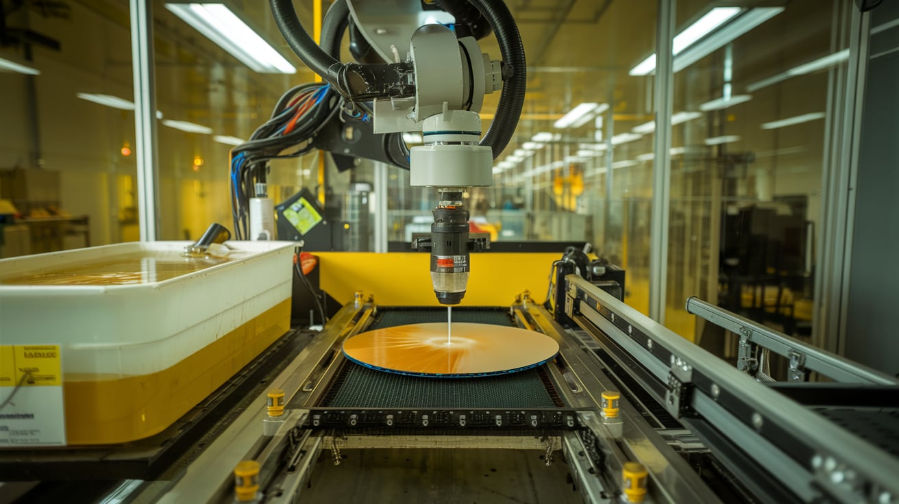
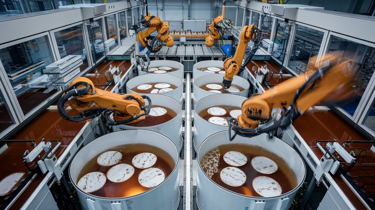
In semiconductor manufacturing, wafer cleaning systems play a critical role in ensuring the cleanliness and precision required for producing high-quality chips. As wafer sizes increase and devices shrink in size, the demand for effective cleaning solutions has grown exponentially. The wafer cleaning system is responsible for removing contaminants such as particles, organic residues, and metal ions from the surface of silicon wafers. Its effectiveness determines the performance and yield of the final semiconductor devices.

This article explores the various features of modern wafer cleaning systems, their drying mechanisms, customizable functionality, and the critical role played by technologies like the spin processor, spin scrubber, and annealing systems in the cleaning process.
Get More Information :
https://www.marketsandmarkets.com/pdfdownloadNew.asp?id=772

1. Features of Wafer Cleaning Systems
Modern wafer cleaning systems come equipped with a variety of features designed to enhance the cleaning process and adapt to the needs of advanced semiconductor manufacturing. These features include:
- Particle Removal: One of the primary objectives of wafer cleaning is the removal of microscopic particles that could interfere with the photolithography process or cause defects in the final semiconductor. Systems use a combination of chemical solutions, water rinses, and physical cleaning to achieve particle-free surfaces.
- Chemical Delivery and Management: Advanced wafer cleaning systems feature precise chemical delivery mechanisms that ensure the right amount of chemicals is applied at the right stage. This reduces chemical waste and improves cleaning efficiency.
- Automated Control Systems: Many cleaning systems today are fully automated, reducing human error and ensuring consistent performance. Automated systems provide precise control over parameters like chemical concentrations, rinse durations, and spin speeds.
- Process Flexibility: These systems can be adapted for different wafer sizes (200mm, 300mm, and larger) and process requirements, making them versatile for various stages of semiconductor production.
- Low Contamination: The cleaning process itself must be contamination-free. Advanced systems incorporate high-purity materials in the design, use closed-loop cleaning solutions, and ensure minimal contamination from the system’s own components.
2. Drying Systems in Wafer Cleaning
The drying stage is a crucial part of the wafer cleaning process as any water or chemical residues left on the wafer can cause defects or contamination. There are several types of drying systems used in wafer cleaning:
- Spin Drying: One of the most common methods of drying wafers is spin drying. After the cleaning process, wafers are spun at high speeds, causing water and cleaning solutions to be flung off by centrifugal force. This method is effective at removing surface moisture without leaving any residue.
- Marangoni Drying: Marangoni drying uses surface tension to remove liquids from the wafer surface. By controlling the chemical gradient at the liquid-air interface, this method allows for the smooth removal of liquid films without leaving any marks on the wafer.
- Vacuum Drying: In some cases, a vacuum drying system is used to evaporate any remaining moisture from the wafer surface. This method ensures that even trace amounts of moisture are removed, which is critical in environments with stringent cleanliness requirements.
Each drying system is chosen based on the specific cleaning application and the sensitivity of the wafer to contaminants or damage during the drying process.
3. Customizable Functionality
Given the complexity of semiconductor manufacturing, wafer cleaning systems must offer customizable functionality to meet the needs of different production lines. Key customizable features include:
- Programmable Cleaning Cycles: Manufacturers can program the system to use different cleaning steps for different wafer types or contamination levels. This allows for flexibility and efficiency in processing diverse materials.
- Adjustable Chemical Mixes: The chemical mix used in wafer cleaning may vary based on the specific contaminants being targeted. Modern systems offer the ability to adjust the chemical mix to optimize cleaning results.
- Modular Design: Many wafer cleaning systems are modular, allowing manufacturers to add or remove cleaning components based on their production needs. This makes it easier to upgrade or modify the system as technology evolves or as production demands change.
- User-Friendly Interfaces: To make these complex systems easier to use, many come equipped with graphical user interfaces (GUIs) that allow operators to control and monitor cleaning processes with ease.
4. Spin Processor Technology
Spin processors are widely used in wafer cleaning due to their efficiency and effectiveness in both cleaning and drying wafers. The process involves placing wafers on a rotating chuck and spraying cleaning solutions or rinses while the wafer spins. The spinning motion ensures uniform coverage of the cleaning agents across the wafer surface while the centrifugal force helps remove contaminants and liquids.
Advantages of spin processors include:
- High Throughput: Spin processing allows for quick and efficient cleaning, making it ideal for high-volume semiconductor manufacturing.
- Controlled Cleaning: The speed of the spin and the amount of chemical applied can be precisely controlled, allowing for tailored cleaning processes.
- Minimal Wafer Handling: Since the wafer remains in place during the process, there is minimal handling, which reduces the risk of mechanical damage or contamination.
5. Spin Scrubber Systems
Spin scrubbers take the concept of spin processing further by adding mechanical scrubbing action to the cleaning process. These systems are equipped with rotating brushes that physically scrub the wafer surface to remove more stubborn contaminants like particles or organic residues. The combination of chemical action and physical scrubbing results in a highly effective cleaning process.
Features of spin scrubber systems include:
- Dual-Brushing Technology: Many spin scrubbers feature dual brushes that scrub both sides of the wafer simultaneously, ensuring comprehensive cleaning.
- Adjustable Pressure and Speed: The pressure applied by the brushes and the speed of rotation can be customized to avoid damaging delicate wafer surfaces while achieving optimal cleaning results.
- Wet and Dry Scrubbing: Some systems offer both wet scrubbing (using cleaning chemicals) and dry scrubbing (using air) to provide flexible cleaning options.
6. Annealing Systems
Annealing is a thermal process that can be integrated into wafer cleaning systems to enhance the removal of certain types of contaminants. By heating the wafer to high temperatures, annealing helps to break down or vaporize contaminants like organic residues or photoresist remnants that cannot be removed through chemical cleaning alone. Annealing systems are often used in conjunction with other cleaning methods to achieve ultra-clean wafer surfaces.
Key benefits of annealing systems include:
- Complete Contaminant Removal: Annealing can target contaminants that are resistant to chemical cleaning, such as stubborn organic compounds or metal oxides.
- Improved Surface Quality: The annealing process can also improve the surface quality of the wafer by eliminating micro-contaminants and smoothing the wafer surface.
- Temperature Control: Advanced annealing systems offer precise control over temperature, ensuring that the wafer is heated to the optimal level without risking damage to the substrate.
Wafer cleaning systems are a cornerstone of semiconductor manufacturing, providing the precision and cleanliness required to produce cutting-edge microchips. Features such as customizable functionality, advanced drying mechanisms, and technologies like spin processors, spin scrubbers, and annealing systems all contribute to the effectiveness of modern cleaning processes. As semiconductor technology continues to evolve, wafer cleaning systems will remain a key enabler in ensuring the production of high-quality, defect-free devices across a wide range of industries.
