The world of semiconductor manufacturing is experiencing a revolutionary shift, with Extreme Ultraviolet (EUV) lithography at the forefront of innovation. This groundbreaking technology is enabling the production of smaller, faster, and more efficient microchips that are essential for powering everything from smartphones and computers to advanced AI systems, autonomous vehicles, and IoT devices. With an ever-growing demand for higher performance and miniaturization, EUV lithography is set to become a critical enabler for the next generation of microchips. In this article, we will delve into the current state of the EUV lithography market, the innovations shaping its future, and the impact it has on semiconductor manufacturing.
What is EUV Lithography?
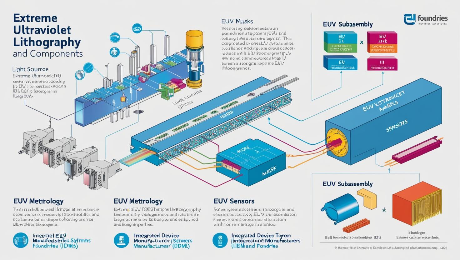
Extreme Ultraviolet (EUV) lithography is an advanced form of photolithography used in semiconductor manufacturing to produce tiny features on microchips. It uses light with a wavelength of about 13.5 nm, which is much shorter than the traditional ultraviolet light used in photolithography (which typically has wavelengths in the range of 193 nm). The shorter wavelength allows EUV lithography to print finer patterns on silicon wafers, enabling the creation of chips with much smaller transistors.
EUV lithography is particularly important as semiconductor manufacturers strive to continue the trend of Moore’s Law, which predicts that the number of transistors on a chip will double approximately every two years. To achieve this level of miniaturization, traditional optical lithography techniques are no longer effective, and EUV offers a solution capable of printing these increasingly smaller features with greater precision.
Market Growth and Adoption of EUV Lithography
The global EUV lithography market has been growing at an impressive pace, fueled by the demand for smaller, more powerful, and energy-efficient chips. According to industry reports, the market is expected to grow significantly in the coming years as major semiconductor players, such as TSMC, Samsung, and Intel, continue to adopt EUV for their next-generation manufacturing processes.
The EUV lithography market is expected to reach USD 22.69 billion by 2029 from USD 12.18 billion in 2024, at a CAGR of 13.2% during the 2024-2029 period.
Key drivers for this growth include:
-
Advanced Semiconductor Manufacturing: As the demand for cutting-edge devices increases, chipmakers are pushing the limits of manufacturing capabilities. EUV lithography is essential for producing chips with node sizes of 7nm, 5nm, and even 3nm, where smaller transistors are required to deliver the enhanced performance expected in modern electronics.
-
Miniaturization of Electronics: From smartphones to smart wearables, consumer electronics are getting smaller and more powerful. EUV lithography allows manufacturers to pack more transistors into a given chip area, improving computational power without increasing the size of the devices.
-
Increased Investment in Research and Development: Major semiconductor manufacturers and equipment providers are investing heavily in EUV technology to improve its efficiency and reduce costs. As these investments continue to bear fruit, EUV will become more accessible, further driving market growth.
Download PDF Brochure @
https://www.marketsandmarkets.com/pdfdownloadNew.asp?id=241564826
Key Innovations Powering the EUV Lithography Market
Several technological innovations are shaping the future of EUV lithography and improving its viability for large-scale semiconductor production. These innovations are focused on enhancing the resolution, speed, and overall efficiency of EUV systems.
1. High-NA EUV Lithography
One of the most significant innovations on the horizon is the development of High-NA (Numerical Aperture) EUV lithography. Traditional EUV systems have a numerical aperture of around 0.33, but next-generation High-NA EUV systems will push this figure to 0.55. This will allow for even finer patterns to be printed on wafers, enabling the production of chips with nodes smaller than 3nm.
The transition to High-NA EUV lithography is expected to open new possibilities for the semiconductor industry, especially in the production of high-performance chips for applications such as artificial intelligence, quantum computing, and 5G.
2. EUV Source Power and Light Generation
One of the challenges of EUV lithography is generating enough light at the right wavelength to perform efficient exposure. Traditional sources of EUV light—plasma-based light sources—have been limited in their power output. However, advancements in laser-produced plasma (LPP) sources and solid-state EUV sources are increasing the intensity and stability of EUV light, making the process more viable for mass production.
By increasing the power of EUV sources, manufacturers can improve throughput, reduce cycle time, and achieve higher yields, making the technology more cost-effective in high-volume manufacturing environments.
3. Advanced Masking and Pellicles Technology
In EUV lithography, masks (which are used to project the chip design onto the wafer) and pellicles (protective layers that prevent contamination of the mask) play a crucial role in achieving high resolution. As the wavelength of light decreases, the precision required for creating and handling masks becomes more challenging.
Innovations in mask manufacturing and pellicle design are addressing these challenges. For example, new pellicle materials that withstand EUV light and are transparent to 13.5 nm wavelength are being developed. Additionally, improvements in mask patterning and defect detection are enabling higher yield rates and reducing defects in chip production.
4. EUV Metrology and Inspection Tools
EUV lithography also requires advanced metrology and inspection tools to monitor the precision of pattern transfer and identify defects at the nanoscale. Companies are developing innovative tools that utilize high-precision optical metrology, electron beam inspection, and atomic force microscopy (AFM) to inspect chips with greater accuracy. These innovations ensure that EUV lithography systems maintain high quality and consistency in production, minimizing defects and improving overall yields.
Impact of EUV Lithography on Semiconductor Manufacturing
The adoption of EUV lithography is transforming the semiconductor manufacturing process in several ways:
-
Faster Time-to-Market: With EUV, manufacturers can produce chips with smaller features more quickly, reducing time-to-market for cutting-edge technologies like 5G and AI applications.
-
Enhanced Chip Performance: EUV lithography enables the creation of smaller transistors, leading to more powerful and energy-efficient chips. These chips can handle more complex tasks, which is critical for the advancement of emerging technologies like autonomous vehicles and the Internet of Things (IoT).
-
Cost and Yield Improvements: While EUV systems are expensive to develop and deploy, their long-term impact is expected to be positive for manufacturers. EUV enables more complex chip designs, improving yield rates and reducing the need for multiple patterning techniques, which can drive down overall production costs.
Challenges and the Road Ahead
Despite its immense potential, the EUV lithography market still faces several challenges:
- High Costs: The cost of EUV machines, along with the need for specialized materials, is still high, which limits accessibility for some smaller manufacturers.
- Technical Hurdles: While significant advancements have been made, EUV technology still faces technical challenges related to source power, mask defects, and throughput that need to be overcome for widespread adoption.
- Supply Chain Issues: As demand for EUV equipment rises, the supply chain for critical components like light sources, masks, and pellicles may become strained, leading to delays and cost pressures.
The EUV lithography market is revolutionizing the semiconductor industry by enabling the production of microchips with increasingly smaller and more powerful transistors. As the demand for high-performance electronics continues to grow, EUV will play a pivotal role in powering the next generation of devices, from smartphones to advanced AI systems. Innovations such as High-NA EUV lithography, improved light sources, and advancements in mask technology are pushing the boundaries of what is possible in semiconductor manufacturing, making EUV an essential technology for the future of electronics. Despite some challenges, the continued evolution of EUV systems promises to transform the way chips are made, unlocking new possibilities for industries and applications worldwide.
Here are some Frequently Asked Questions (FAQ) related to the EUV Lithography Market:
1. What is EUV Lithography?
Extreme Ultraviolet (EUV) Lithography is a cutting-edge semiconductor manufacturing technology that uses light with a wavelength of 13.5 nm, which is much shorter than the conventional ultraviolet light used in traditional photolithography. This enables the production of smaller and more powerful transistors, essential for next-generation microchips in electronics.
2. Why is EUV Lithography Important for Semiconductor Manufacturing?
EUV lithography is essential for pushing the boundaries of Moore’s Law, which predicts the doubling of transistors on microchips every two years. With shorter wavelengths, EUV allows the creation of smaller transistors at more advanced nodes (e.g., 5nm, 3nm), enabling the manufacturing of faster, more efficient microchips used in smartphones, AI, IoT, and more.
3. What Are the Key Benefits of EUV Lithography?
- Smaller Transistors: EUV enables the creation of chips with smaller nodes, leading to increased computational power and energy efficiency.
- Enhanced Performance: EUV helps create more powerful chips for advanced applications like AI, 5G, and quantum computing.
- Faster Time-to-Market: EUV reduces the time required for patterning, speeding up chip production.
- Cost-Efficiency: Though initially expensive, EUV can lower production costs in the long run by eliminating the need for multi-patterning techniques.
4. What Are the Challenges of EUV Lithography?
- High Costs: EUV machines and the associated equipment are expensive, which makes it a challenge for smaller manufacturers to adopt this technology.
- Technological Limitations: Challenges related to the power of EUV light sources, mask defects, and throughput need to be overcome for widespread adoption.
- Supply Chain Issues: The complexity of the technology and the need for high-precision components can cause delays in the supply chain and increase costs.
5. Which Companies Are Leading the EUV Lithography Market?
Key players in the EUV lithography market include:
- ASML: The primary supplier of EUV lithography machines, ASML is at the forefront of advancing this technology.
- Samsung and TSMC: These semiconductor giants are leading the adoption of EUV in chip production for smaller nodes.
- Intel: Intel is also working on integrating EUV into its manufacturing processes as it pushes forward with cutting-edge semiconductor production.
6. What are High-NA EUV Lithography Systems?
High-NA EUV (Numerical Aperture) lithography is the next generation of EUV systems. It features a higher numerical aperture (NA) of 0.55 compared to the current EUV systems with an NA of 0.33. High-NA EUV will allow for the creation of even smaller and more precise features on chips, essential for future nodes (like 2nm or smaller) and advanced chip designs.
7. How is EUV Lithography Changing the Semiconductor Industry?
EUV lithography is enabling the production of smaller, more powerful, and energy-efficient microchips that power cutting-edge technologies such as AI, 5G, autonomous vehicles, and smart devices. It’s facilitating faster chip production, improving yield rates, and reducing multi-patterning costs, ultimately transforming the semiconductor manufacturing process and expanding the capabilities of modern electronics.