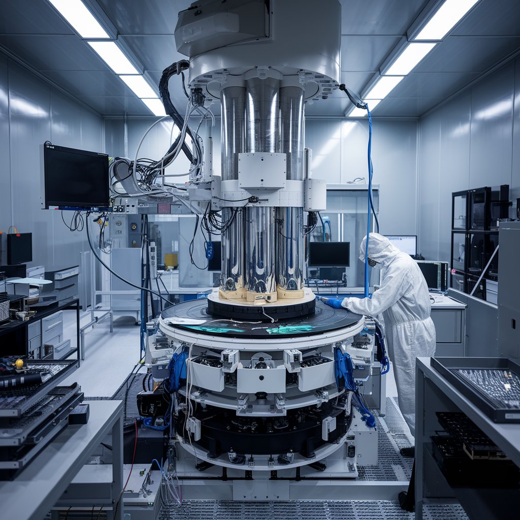
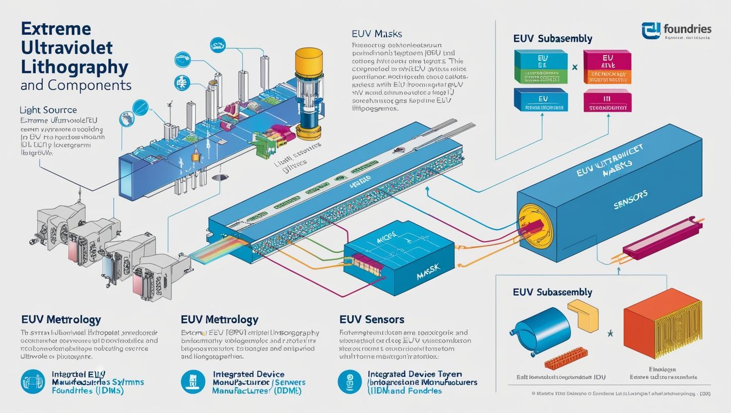
As the demand for smaller, faster, and more powerful semiconductors continues to surge, Extreme Ultraviolet Lithography (EUVL) stands at the forefront of the revolution in semiconductor manufacturing. This advanced technology is set to redefine the capabilities of the semiconductor industry, allowing manufacturers to meet the ever-growing need for high-performance chips that power everything from smartphones to artificial intelligence (AI) systems and autonomous vehicles.
EUVL is rapidly becoming a cornerstone of the semiconductor manufacturing process, playing a pivotal role in producing chips at smaller node sizes, which are crucial for enhancing the performance, efficiency, and functionality of modern electronic devices. This article delves into the future of EUVL, its impact on the semiconductor industry, and the trends that will shape its growth.
What is Extreme Ultraviolet Lithography (EUVL)?
Extreme Ultraviolet Lithography (EUVL) is a cutting-edge photolithography technique that uses extreme ultraviolet light with wavelengths as short as 13.5 nanometers to create patterns on semiconductor wafers. These patterns form the intricate circuits that are etched onto silicon chips. EUVL is a critical enabler for manufacturing chips with extremely small transistors, enabling the production of advanced semiconductor nodes, such as 7nm, 5nm, and the upcoming 3nm nodes.
Unlike traditional photolithography, which uses light sources with longer wavelengths, EUVL’s shorter wavelengths allow for finer patterning at higher resolutions, making it indispensable for modern chip production. The technology is being heavily invested in by leading semiconductor manufacturers, as it is vital to keep pace with the relentless progression of Moore’s Law, which predicts that the number of transistors on a chip will double approximately every two years.
The Role of EUVL in Semiconductor Manufacturing
EUVL has emerged as the solution to many of the challenges semiconductor manufacturers face when scaling down transistor sizes. To produce advanced semiconductor nodes, traditional photolithography methods, such as Deep Ultraviolet Lithography (DUV), are unable to achieve the required resolutions. EUVL solves this problem by providing the capability to pattern structures at much smaller scales, enabling the production of chips with improved performance and reduced power consumption.
The transition to smaller nodes is essential for meeting the growing demand for higher processing power in consumer electronics, cloud computing, and emerging technologies like 5G, AI, quantum computing, and autonomous systems. EUVL also enables the production of chips with more transistors per unit area, driving the miniaturization of electronic devices.
Future of extreme ultraviolet lithography (euvl) industry include
The EUV lithography market is expected to reach USD 22.69 billion by 2029 from USD 12.18 billion in 2024, at a CAGR of 13.2% during the 2024-2029 period.
Key Drivers of Growth for EUVL
1. Advancements in Chip Technology and Demand for Smaller Nodes
As semiconductor manufacturers push towards 5nm and 3nm process nodes, the ability to print increasingly smaller patterns on silicon wafers is becoming crucial. The scaling of transistor sizes allows for higher performance, lower power consumption, and increased efficiency. EUVL is the key technology to achieving these smaller nodes, particularly for the most advanced chips in the market.
The introduction of 5G networks and the rise of artificial intelligence (AI) applications have created a demand for semiconductors with enhanced processing capabilities. The need for chips that can handle massive amounts of data and perform at high speeds will drive continued investment in EUVL.
2. Increased Adoption of High-Performance Computing and AI
The demand for high-performance computing (HPC) and AI-based technologies is another major growth driver for EUVL. These technologies require specialized chips that are both powerful and energy-efficient. EUVL enables manufacturers to produce chips with the advanced architectures needed to support AI workloads and data center applications, which require cutting-edge semiconductor technology to handle large-scale computations.
The ever-expanding applications of AI—from autonomous vehicles to cloud services and machine learning—require semiconductor chips that offer significant performance improvements. EUVL helps meet this demand by enabling the production of highly complex and compact chips, which are essential for AI applications to operate at scale.
Download PDF Brochure @
https://www.marketsandmarkets.com/pdfdownloadNew.asp?id=241564826

3. Moore’s Law and the Push for Continuous Scaling
Moore’s Law, which states that the number of transistors on a chip doubles approximately every two years, has driven semiconductor innovation for decades. However, as transistor sizes shrink below the 10nm threshold, manufacturers face increasing challenges in maintaining the pace of Moore’s Law. EUVL has emerged as a critical tool to help manufacturers continue scaling down semiconductor nodes and producing chips with smaller transistors.
EUVL’s capability to produce smaller features and more intricate patterns on chips is central to ensuring that Moore’s Law remains relevant in the age of advanced semiconductor fabrication. The technology enables companies to continue pushing the boundaries of performance and efficiency in microelectronics.
Challenges and Innovations in the EUVL Market
Despite its groundbreaking potential, EUVL still faces several challenges. One of the most significant challenges is the cost. The development and deployment of EUVL systems are expensive, with each machine costing hundreds of millions of dollars. The complexity of EUVL systems, including the need for extremely precise mirrors, light sources, and photoresists, further adds to the cost.
However, with continued technological advancements and economies of scale, these costs are expected to decrease over time. The industry is already witnessing increased investments in EUVL by major semiconductor companies such as TSMC, Intel, and Samsung, who are working on refining the technology and improving its cost-effectiveness.
Another challenge is the lack of sufficient availability of EUV lithography machines, which are currently dominated by ASML, the only supplier of high-volume EUV lithography machines. As demand for these machines grows, there will be increased competition to secure these resources, leading to potential supply chain bottlenecks.
Despite these challenges, innovations in the EUVL market are paving the way for its widespread adoption. For example, extreme ultraviolet (EUV) light sources are becoming more powerful and stable, making the process more efficient. Additionally, photoresist materials are continuously being developed to optimize the EUVL process and improve resolution accuracy.

The Road Ahead: EUVL’s Impact on Future Semiconductor Manufacturing
Looking ahead, EUVL is poised to play a vital role in the future of semiconductor manufacturing. As the industry moves toward 2nm and 1nm process nodes, EUVL will be indispensable for ensuring that transistors continue to shrink without compromising performance or energy efficiency. The ongoing investment in EUV infrastructure and research will continue to unlock new possibilities for chip manufacturing, helping to meet the growing demand for faster, more efficient, and compact chips.
In addition, EUVL will drive the development of advanced packaging technologies and 3D integration. These advancements will allow for even greater levels of integration and miniaturization in chips, leading to the creation of more sophisticated electronics across a wide range of industries.
Extreme Ultraviolet Lithography (EUVL) represents a transformative leap forward in semiconductor manufacturing. As the industry pushes toward smaller nodes and more advanced chips, EUVL will continue to play a central role in enabling the production of the next generation of high-performance semiconductors. While challenges remain, the future of EUVL is bright, with significant innovations and investment driving its evolution.
The technology will unlock new opportunities for industries ranging from consumer electronics to cloud computing and artificial intelligence, allowing for faster, more powerful, and more energy-efficient devices. As EUVL technology continues to mature, it will revolutionize semiconductor manufacturing and help shape the future of electronics and computing.
Frequently Asked Questions (FAQ) about Extreme Ultraviolet Lithography (EUVL)
1. What is Extreme Ultraviolet Lithography (EUVL)?
Extreme Ultraviolet Lithography (EUVL) is a photolithography technique used in semiconductor manufacturing. It utilizes extreme ultraviolet light with a wavelength of 13.5 nm to print tiny patterns on silicon wafers. This process is essential for producing advanced semiconductor chips with smaller transistors, enabling the development of smaller, faster, and more energy-efficient devices.
2. How does EUVL work?
EUVL works by directing extreme ultraviolet light onto a photosensitive layer on a silicon wafer. The light is passed through a mask, creating patterns that define the circuitry for semiconductor chips. The smaller wavelength of EUV light enables the production of finer patterns, which are essential for fabricating chips at smaller process nodes, such as 7nm, 5nm, and 3nm.
3. Why is EUVL important for semiconductor manufacturing?
EUVL is crucial for producing next-generation semiconductor chips that are smaller, faster, and more efficient. Traditional photolithography methods, like Deep Ultraviolet Lithography (DUV), cannot achieve the resolution needed for advanced nodes. EUVL’s shorter wavelength allows it to pattern features with higher precision, supporting the industry’s drive to create smaller transistors and increase chip performance while reducing power consumption.
4. What are the benefits of using EUVL in chip production?
The main benefits of EUVL include:
- Higher resolution: Enables the production of smaller and more intricate features on chips.
- Smaller transistors: Facilitates the scaling down of transistors, increasing the number of transistors per chip and improving overall performance.
- Improved efficiency: Supports the development of more energy-efficient chips, essential for devices like smartphones, AI systems, and cloud computing.
- Moore’s Law: Helps continue the advancement of Moore’s Law, allowing for further miniaturization of electronic devices.
5. What industries benefit from EUVL?
EUVL is benefiting industries that rely on advanced semiconductor chips, including:
- Consumer electronics (smartphones, tablets, laptops)
- Artificial intelligence (AI)
- Cloud computing
- Automotive (self-driving cars, electric vehicles)
- Telecommunications (5G networks)
- Medical devices and wearables
